Advanced Power Device Design
Innovative Device Architecture
Structural Optimization
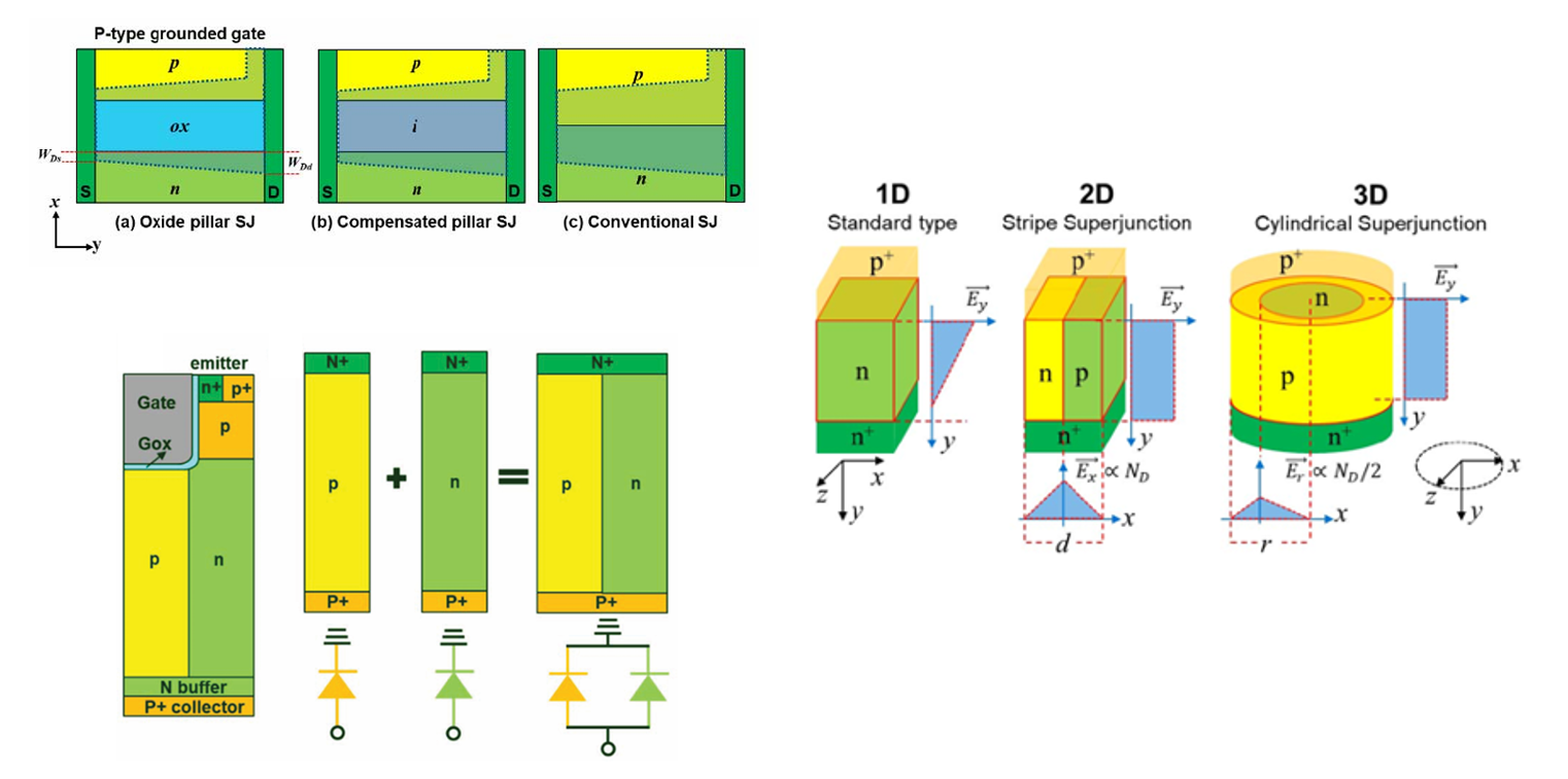
- Structural Optimization for Next-Generation Devices
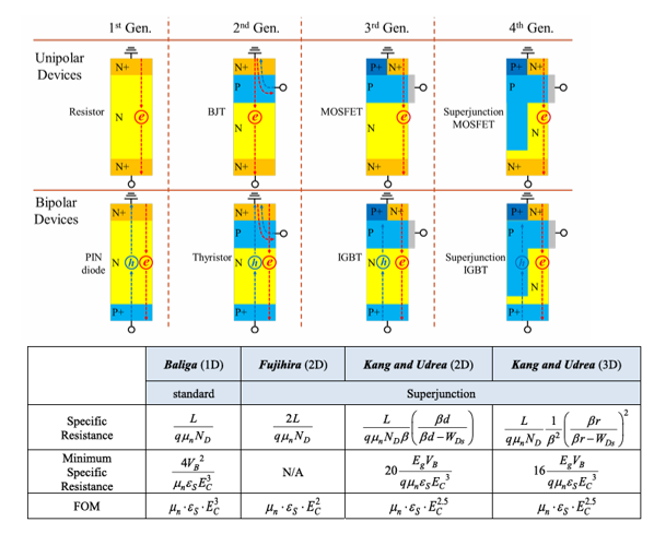
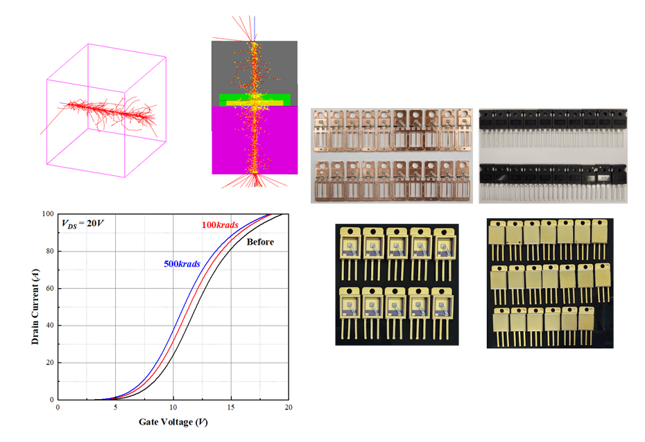
We explore novel device architectures designed to overcome the inherent trade-offs of conventional structures. By introducing advanced structural concepts—such as optimizing pillar geometries and incorporating dielectric materials—we minimize parasitic effects and maximize the performance figure of merit, achieving a superior balance between breakdown voltage and on-state resistance.
Moving beyond traditional planar and 2D limitations, we investigate device architectures across multiple dimensions. By analyzing electric field distributions in 3D space, we design structures that enhance the depletion region and allow for higher doping concentrations, thereby significantly reducing on-state resistance.
Process Variation
- Impact of Process Variation
We analyze how manufacturing realities, such as Pillar Ripple (doping fluctuation), affect device performance. Our work quantifies the trade-offs between static efficiency ($R_{sp}$) and dynamic stability (Gate Ringing, $E_{off}$), offering practical design guidelines to balance performance with ruggedness.
Physics-Based Modeling & Simulation
Process Simulation
- Process Simulation
We simulate actual semiconductor fabrication steps—such as ion implantation, diffusion, etching, and deposition—to generate accurate doping profiles and device structures. Key structural features, including pillar ripple formation and junction depth, are determined at this stage.
Device Simulation
- Device Simulation
Based on the fabricated structure, we apply external bias conditions and solve the Poisson equation together with the carrier continuity equations. This enables a physics-based analysis of I–V characteristics, electric-field distribution, and impact ionization behavior. Beyond observing simple trends, our focus is on calibrating physical models—including mobility degradation, Shockley–Read–Hall recombination, and other advanced mechanisms—to ensure close agreement with real device behavior.
Mixed Mode Simulation
- Mixed Mode Simulation
Single-device characteristics alone cannot explain the transient behavior observed during high-speed switching. This approach enables detailed analysis of gate ringing caused by the interaction between parasitic gate inductance, parasitic source inductance, and the device's input capacitance. It also allows extraction of dynamic gate-to-drain capacitance and dynamic drain-to-source capacitance under realistic high-dV/dt switching conditions.
SPICE Modeling
- SPICE Modeling & Application
We bridge the gap between physical device characteristics and circuit-level performance using LTspice and PSpice. By developing precise compact models that reflect both static and dynamic behaviors—including non-linear capacitance and temperature dependencies—we enable accurate system-level simulations. By coupling device physics with circuit elements, we analyze gate ringing caused by parasitic inductances and input capacitance interactions.
Theoretical Limit & FOM Analysis
True Material Limit
- True Material Limit
We challenge conventional wisdom by identifying the "True Material Limit" of power devices. Unlike ideal models that suggest indefinite scaling, our analytical approach incorporates the parasitic JFET effect and depletion-width modulation to determine the fundamental lower bound of specific on-state resistance for Si and SiC.
New FOM
- New Figure of Merit (FOM)
We establish new Figures of Merit that accurately reflect the potential of superjunction devices. By deriving the optimum cell pitch and doping concentration as a function of material properties (Bandgap, Critical Electric Field), we provide a rigorous theoretical framework for next-generation device design.
Comprehensive Device Characterization
- Static & Thermal Characterization
Static & Thermal
We perform comprehensive static analysis using high-power curve tracers and probe stations capable of handling ultra-high voltages and currents. Beyond standard I-V measurements (Breakdown Voltage, On-resistance, Leakage), we characterize device behavior across extreme temperature ranges—from cryogenic to elevated temperatures—to ensure thermal stability and reliability in harsh operating environments.
- Dynamic & Switching Characterization
Dynamic & Switching
Conventional small-signal capacitance measurements often fail to predict real-world switching behavior. We specialize in extracting and analyzing non-linear parasitic capacitances (Ciss, Coss, Crss) under high-voltage bias conditions. Also, we evaluate transient performance through advanced Double Pulse Testing (DPT) with optimized low-inductance board designs.
- Ruggedness Characterization
Ruggedness
To ensure device reliability under fault conditions, we push devices to their physical limits to define the Safe Operating Area (SOA). We conduct destructive and non-destructive tests, including Short-Circuit (SC) capability, Unclamped Inductive Switching (UIS) for avalanche robustness, and Surge Current (IFSM) tests, verifying that devices can withstand extreme electrical stresses in real-world applications.
Module, System & Reliability
- Reliability Physics & Robustness
Reliability
We conduct rigorous reliability assessments based on automotive-grade standards such as AEC-Q101 and AQG-324. Our research focuses on accelerated lifetime testing (ALT), including High-Temperature Reverse/Gate Bias (HTRB/HTGB), High-Humidity High-Temperature Reverse Bias (H3TRB), and Power Cycling tests, to predict long-term device stability under thermal and electrical stress.
- Failure Analysis & System Integration
Failure Analysis
We employ a multi-faceted approach to failure analysis to identify root causes of device degradation. This includes non-destructive techniques like Scanning Acoustic Microscopy (SAT) for delamination detection and Photoemission Microscopy (EMMI) for leakage path localization, as well as destructive physical analysis (DPA) methods like decapsulation and cross-sectioning.